
In the final post, we will take our investigation one step further to gain runtime control of the TEE kernel. We will show how the kernel exposes a driver that can be used by privileged TAs to map physical memory into the TA memory space. We will leverage this driver from the HDCP TA to map secure registers and unprotect the TEE memory. Finally, we will use the same HDCP TA to modify the hypervisor page tables and allow Android apps to map the (now unprotected) TEE memory with complete read/write access.
In the past, functionality to directly map physical memory into a TA has been a common weakness that has been targeted for exploits in TEEs, as explained here. In the case of the S7, the issue lied in the fact that the kernel did not perform enough checks on the physical memory area to be mapped in the TA, allowing mapping sensitive locations such as the EL3 code into a TA memory.
It, therefore, made sense for us to look at how TEEGRIS implements this and see if similar vulnerabilities are present. We quickly identified a driver that runs in the kernel, accessible through “phys://”.
Figure 1. phys handler registration
The phys driver is very similar to the “/dev/mem” Linux device, and is accessible with a few syscalls, the most interesting ones being open and mmap. The open syscall handler for phys:// does the following:
Figure 2. TA permissions check in the open syscall handler
In lines 9-13, the code checks that the TA has rights to map at least one of the 5 possible areas: internal RAM, internal boot ROM, secure DRAM, non-secure DRAM, and registers. If so, the function will succeed.
In part 1 of our blog post, we showed that the permissions are statically assigned to each group. The HDCP TA in which we have runtime control is, fortunately, part of the highly privileged “samsung_drv” group, which can access the phys driver. In fact, the TA needs the phys driver for one of its commands, so it makes sense for the HDCT TA to belong to the “samsung_drv” group.
Now that we know that the driver can be accessed by the TA, we can analyze the mmap handler and see what kind of checks are in place.
Figure 3. phys mmap handler
In line 16 of Figure 3, function get_memory_type is called passing the provided range as argument. Value “1” is then shifted left by the return value of the get_memory_type function. In the rest of the code, we see that the function checks whether the resulting value is 8 (corresponding to non-secure RAM, highlighted in green in the picture), 16 (meaning registers, highlighted in red), or 1 (ROM, highlighted in blue). It seems secure RAM and internal RAM (where the EL3 code runs) can never be mapped inside a TA, even though they exist in the list of permissions that TAs can have.
Without going into the details of the get_memory_type function, it seems that only non-secure RAM and registers can be mapped in the HDCP TA since the group samsung_drv does not have permissions to map the ROM. Out of the two regions, non-secure RAM is of limited interest. It could be abused for privilege escalation in the REE (in fact, it was possible in another TA, see SVE-2019-15873), but we are interested in the TEE, which fully resides in secure RAM. On the other hand, registers are more interesting from an attacker’s point of view since they contain all the registers used to configure peripherals, including the ones used for configuring TrustZone.
Now that we knew what we wanted to access, it was time for creating a Return Oriented Programming (ROP) payload that would allow us to map and access these memory areas. To do so, we opted to create a generic physical to physical memory copy payload that does the following:
- Open a handle to the phys driver
- Invoke mmap twice to map the source and destination buffers
- Jump to memcpy
This primitive can be used both to read out registers (by setting the memcpy source to a register memory and the destination to non-secure memory) or to modify them (by setting the memcpy source to non-secure memory and the destination to a register) from an Android app.
After implementing the ROP payload, it was time to decide what exactly we wanted to copy and where.
ION buffers
As a first step, we had to find a way of sharing physical memory between our CA running on Android and our compromised HDCP TA running on the TEE. This is not straightforward because normally, a regular Android application has no way of knowing at which physical address a buffer is mapped.
For this purpose, we used a mechanism provided by Android called ION, which is basically a shared memory manager aimed at eliminating memory copies when sharing data between two entities. These buffers can be accessed from Android apps, so we could use them from our client application. The allocator guarantees that memory will be mapped at a known physical address. The subsystem can be accessed by interacting with /dev/ion, which allows performing an open call to get a file descriptor and then ioctls to request an ION buffer.
We downloaded the Android sources corresponding to the firmware version of one of the devices, released by Samsung, and found an ION buffer which would suit our purposes by looking into the Device Tree Sources (DTS). The following snippet of the file called exynos9820-beyond0lte_common.dtsi contains certain details regarding this buffer such as the start address (0x99000000) and the size (0xE400000):
camera {

compatible = "exynos9820-ion";

ion,heapname = "camera_heap";

reg = <0x0 0x99000000 0xE400000>;

ion,recyclable;

};
This means that if we map the whole camera_heap ION buffer in our CA and map physical address 0x99000000 in the HDCP TA, we should have two views of the same memory.
Modifying the TZASC
After solving this, the only remaining piece of the puzzle was finding out what registers to map and at which location they are mapped. In part 1 of this series, we mentioned two registers that are commonly used for configuring TrustZone: TZASC and TZPC. If a TA could access any of them, it would be possible to read the contents of such registers but also write to them, allowing to unprotect memory regions or peripherals. In principle, modifying any of the two could allow the REE to access the TEE, effectively compromising the security provided by the TEE. However, in our experience targeting the TZASC is easier since the TZPC structure is device-dependent (and there is no public documentation for the Exynos chip that powers the S10), while the TZASC is more or less standardized.
By reversing the TEEGRIS kernel code, we found functions related to the TZASC handling, which allowed us to learn that there are, in fact, 4 TZASC peripherals in this SoC (presumably one per DRAM controller).
We started by searching for the string “tzasc” and seeing if we had a hit within the TEE kernel binary. This is how we reached the initialization function in the next figure, which gave us the address of the TZASC handler.
Figure 4. TZASC driver initialization
The “dev://tzasc” device is accessible using the ioctl syscall that ultimately calls tzasc_get_settings_for_range.
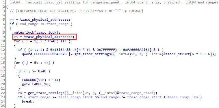
Figure 5. Decompiled tzasc_get_settings_for_range
Even though the exact purpose of this function is not interesting for our attack, we noticed that it references a structure that we named tzasc_physical_addresses, which contains what we suspected are the physical addresses of the 4 different TZASC peripherals.

Figure 6. Physical addresses of the 4 TZASC peripherals
In order to validate our assumptions, we correlated this information with the physical memory map for each physical device we gathered from Android by reading /proc/iomem. The idea behind this validation was that the TEE physical ranges should not overlap with the REE ones. The following listing shows that there are gaps between the REE mcinforegister locations, which leave space for the TZASC registers. Note that the “TZASC” strings were added manually to facilitate reading the output and are not present in the normal iomem output.
beyond0:/data/local/tmp # cat /proc/iomem

…

1bc3004c-1bc3004f : /mcinfo@1BC300000

-----TZASC1:0x1BC40000-----

1bd3004c-1bd3004f : /mcinfo@1BC300000

-----TZASC2:0x1BD40000-----

1be3004c-1be3004f : /mcinfo@1BC300000

-----TZASC3:0x1BE40000-----

1bf3004c-1bf3004f : /mcinfo@1BC300000

-----TZASC4:0x1BF40000-----
After gathering all the required information, we could finally try to see if the exploit worked. We first attempted to read out the TZASC contents. To do so, we followed these steps:
- Have an Android app that maps the camera_heap buffer and initializes it to a fixed, known value.
- In parallel, exploit the HDCP TA to do a physical to a physical memory copy of 0x1000 bytes (the size of the TZASC register set) from 0x1BC40000 (the address of the first TZASC) to 0x99000000 (the address of the camera heap).
- In the Android app, continuously monitor the camera heap. If its contents changed, the TA exploit execution succeeded.
- Save the buffer contents to a file for further analysis.
Indeed after a few seconds, the execution was completed, and a dump of the TZASC was saved to a file. We, therefore, opened the dump and analyzed it using a hex editor:
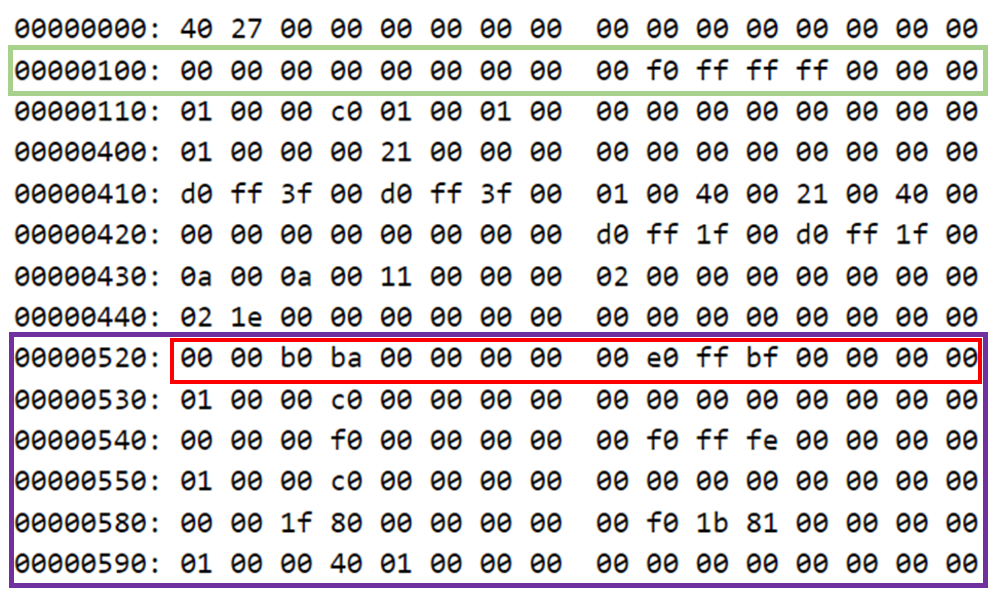
Figure 7. Dump of the TZASC ranges
The configuration of the four TZASC controllers in the system is very similar, therefore, we include only one as the same applies to the others. The green box in the picture denotes region 0, which is the default base region as explained in Part 1 of our series (0x0000000000000000-0x000000fffffff000), whereas the purple frame comprises all the secure ranges configured in the system at a certain moment in time. Each secure range contains two times 8 bytes (little endian) which denote the start and end address, respectively, and then 16 more bytes for the attributes. Finally, the area highlighted in red shows the start and end address of the secure range, which belongs to the TEE OS (0x00000000bab00000- 0x00000000bffff000). This matches with the information provided by /proc/iomem:
80000000-baafffff : System RAM

80090000-8197ffff : Kernel code

82380000-831b0fff : Kernel data

c0000000-dfffffff : System RAM
As can be seen, a gap is left for the TEE area since that memory is not accessible to the REE.
As a next step, we then slightly changed the exploit code to overwrite the 4 TZASCs instead of reading them. The same physical to physical ROP payload can be used, but the source and destination addresses are swapped. We targeted the start address of the secure range for the TEE OS, and we set it to a value larger than the end address. This makes the range invalid, which means it is ignored, and the whole TEE memory is effectively configured as non-secure.
Accessing the TEE memory
At this point, we have a running system in which the whole TEE memory is non-secure and therefore accessible to the REE. This leaves us with the last hurdle: how to access that memory?
As shown before, the HDCP TA cannot access it because the phys driver will deny access to secure memory (even though the range is now reconfigured as non-secure). Therefore, it has to be accessed from the Android app. However, in no normal circumstance, the Linux kernel would allow mapping this range, as it is reserved for the TEE. Therefore, we had to find a way around this issue by keeping in mind that the TA can still access the whole non-secure memory through our exploit.
A number of options are possible, and, in the end, we decided to do this by leveraging Samsung’s hypervisor: RKP (refer to part 1 of our blog post series for an introduction to ARMv8-A privilege levels). Samsung provides the following diagram to explain one of the implemented security features:
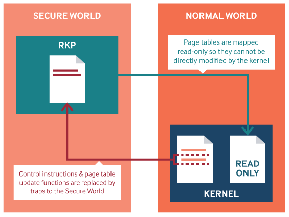
Figure 8. RKP read-only page protection
When a hypervisor is present in an ARMv8-A system, there is another stage of translation tables, originally meant to allow the system to have more than one guest operating systems. The translation process is therefore comprised of two stages. The Linux kernel performs the first step and goes from a virtual address to what is called an Intermediate Physical Address (IPA). The hypervisor takes the IPA and finally translates it to the final Physical Address (PA).
The following picture, taken from here, explains the 2-stage memory translation process.
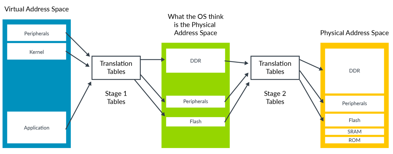
Figure 9.
The memory permissions can be restricted by the hypervisor, meaning that if a certain page is mapped as, e.g., read-only in the second stage, the Linux kernel has no way to modify its contents, even if the page is mapped with write permissions within the kernel itself. With RKP, this is used to enforce that certain security-sensitive structures in the Linux kernel memory are read-only and cannot be modified even if an attacker has arbitrary code execution in the kernel context.
The idea of our attack is then finding the hypervisor’s translation tables corresponding to the camera_heap ION buffer and changing them to point to the TEE kernel physical addresses. Note that gaining access to the TEE memory could also be done by modifying structures within the Linux kernel itself and ignoring the hypervisor, however, we expected targeting the hypervisor to be easier due to the fact that it is significantly less complex compared to the Linux kernel. We presumed that the stage 2 page tables would be mapped at a fixed physical address and never modified, and therefore we would not need to parse complex structures to find which exact memory location needs to be modified.
To confirm if our hypothesis was true, we had to find and extract the hypervisor memory in the system RAM. In order to have information about the memory layout of the system, we dumped the /proc/iomem information, which revealed three main RAM ranges. We used our exploit to dump the physical memory corresponding to each of the ranges and then searched for strings such as “RKP”. The search revealed that the hypervisor starts at physical address 0x87000000as part of the first RAM range.
The second task was to find the page table entries corresponding to the camera_heap ION buffer within the hypervisor’s memory.
In principle, we could have disassembled the binary of the hypervisor to look for how the TTBR registers are initialized and parse the tables. However, since we had a runtime dump of the hypervisor memory, we decided to inspect it to try and find the page tables directly. Knowing how the page tables look like allowed us to scan the memory and recognize them. ARM’s documentation on address translation for ARMv8-A explains how the translation table descriptors look like both for the block entries and for the table entries. The following figure depicts how a block entry looks like:
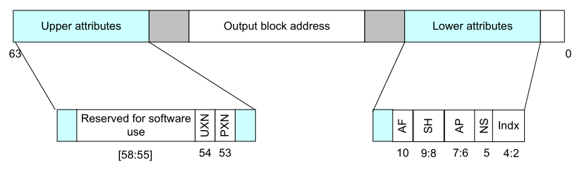
Figure 10. Structure of a block page table entry
We went back to our memory dump with this information and found the block entries corresponding to our ION buffer depicted in the following figure.
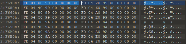
Figure 11. Block entries for the camera_heap buffer
In the highlighted example, the entry is set to 0x990004FD (in little endian). Since we are only interested in changing the address, the attributes can be ignored, and the output block address thus becomes 0x99000000, corresponding to the address of the camera heap.
The last step in the process was to modify our exploit payload, such that the page table entries for our camera heap would be replaced with the ones of the TEE kernel. This way, when accessing the camera heap from the REE, the CA would actually be accessing the TEE memory. For this, we divided the secure range into 2MB increments (the size of each block page table entry) and kept the lower bytes that hold the attributes as they were set for the camera heap (i.e.: FD 04).
Doing this lead to a successful dump of the secure range, inside of which we found several binaries such as shared libraries, loaded TAs (including the HDCP TA we used for the exploit), and the TEE kernel itself. As the memory is now mapped in the REE using page tables under our control, there are no limitations in the pages’ permission, meaning that all the memory, including code, is writable. All modifications will be reflected in the view that the TEE has of the same memory.
To summarize, in order to be able to gain full access to the TEE memory, we had to chain a number of vulnerabilities:
- A missing GP parameters check in the HDCP TA allowed us to obtain arbitrary read/write within the TA.
- A stack-based buffer overflow could be leveraged to then gain arbitrary code execution in the TA context.
- Antirollback is not used for TAs, meaning that even though Samsung correctly fixed the TA vulnerabilities, we could still load the old vulnerable TA.
- Group-based permissions are sometimes too coarse, as the HDCP TA was allowed to map registers even though it only needs access to non-secure memory.
- For TAs that were allowed to access registers, the kernel would allow mapping of registers such as TZASC and TZPC. These registers can be used to compromise the security provided by the TrustZone technology completely, and therefore should never be accessible to TAs.
Conclusions
This concludes the full chain of exploits. At this stage, we managed to map all the TEE memory into an Android application. The memory is fully readable and writable; this means that it is possible to:
- Modify the code of TAs and TEE kernel since the permissions restrictions do not apply to the Android application.
- Bypass countermeasures implemented in the kernel such as KASLR, PAN, and PXN. KASRL is trivially bypassed due to the fact that we have arbitrary read, while other countermeasures do not have an impact since memory can be directly read and written.
Once an attacker has full control of the TEE, a number of attacks can then be performed, such as modifying the phone unlock functionality implemented in the TEE (fingerprint or face recognition) to bypass the screen lock.